")
Vias are a crucial component in printed circuit board (PCB) design, playing a significant role in establishing electrical connections between different layers of the board. This blog will delve into the various types of vias, their functions, and best practices for incorporating them into your PCB designs.
What is Via in Pcb?

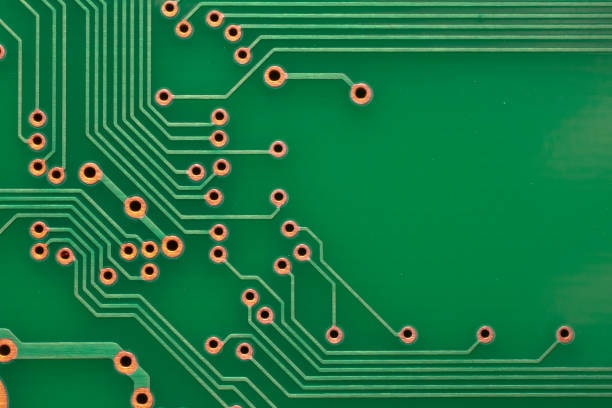
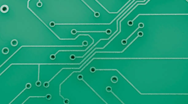
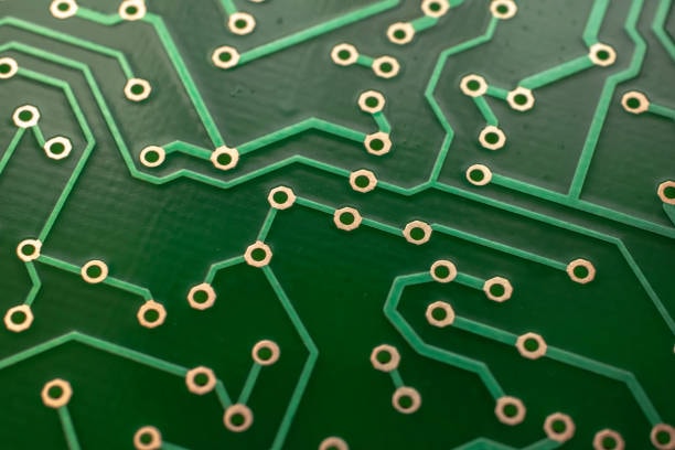
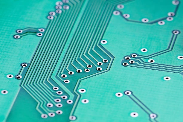
In printed circuit board (PCB) design, a via is a small hole drilled through the board that allows electrical connections to be made between different layers of the PCB. Vias are filled or plated with conductive material, typically copper, to create an electrical pathway. They are essential for multi-layer PCBs, enabling the complex interconnections needed for modern electronic devices. Vias come in various types, including through-hole vias (which pass through the entire board), blind vias (which connect outer layers to inner layers without going through the entire board), and buried vias (which connect inner layers only). Each type of via serves specific purposes and is used based on the design requirements of the PCB.
Via Covering Process
The via covering process in PCB design involves methods used to protect or enhance vias, the small holes that provide electrical connections between different layers of the board. There are several techniques for covering vias, each with specific applications and benefits:
Tenting
Tenting covers the via with a layer of solder mask, a protective coating applied over the PCB. The solder mask prevents solder from flowing into the via during the assembly process. Tenting is commonly used for smaller vias and provides basic protection.
Plugging
Plugging involves filling the via with a non-conductive or conductive material, such as epoxy. This process ensures that the via is sealed and can enhance the board’s mechanical strength. Conductive plugs can also help improve thermal and electrical performance.
Capping
Capping, or via-in-pad, is when vias are placed directly beneath component pads and then filled and capped with copper. This technique ensures a flat, smooth surface, essential for high-density designs and improving component placement and solder joint reliability.
Overplating
Overplating involves adding an extra layer of copper over the filled via, providing additional strength and improving electrical conductivity. This method is often used in high-frequency and high-current applications where enhanced performance is needed.
Backdrilling
Backdrilling is a technique used to remove the unused portion of a via, reducing the stub effect and improving signal integrity, especially in high-speed applications. The process involves drilling out the non-functional part of the via, leaving a clean connection.
Benefits of Via Covering
- Enhanced Reliability: Covered vias are less prone to physical damage and contamination, increasing the overall reliability of the PCB.
- Improved Performance: Filling and capping vias can improve thermal and electrical conductivity, crucial for high-performance applications.
- Solder Joint Quality: Preventing solder from wicking into vias ensures better solder joints and component placement.
- Design Flexibility: Advanced via covering techniques allow for more compact and complex PCB designs, accommodating high-density components and intricate routing.
The Different Types of Vias and Their Applications
Vias are an essential component in printed circuit boards (PCBs), allowing for electrical connections between different layers. Understanding the different types of vias and their applications is crucial for effective PCB design, especially as designs become more complex and compact. Here, we’ll explore the three main types of vias: through-hole vias, blind vias, and buried vias, along with their specific applications.
Through-Hole Vias
Description
Through-hole vias are the most common type of via, extending from the top layer to the bottom layer of the PCB. They penetrate all layers of the board, providing a direct electrical connection between them.
Applications
- Single and Double-Layer PCBs: Used in simpler designs where layers are minimal.
- Multi-Layer PCBs: Employed when connections across multiple layers are required.
- Power and Ground Connections: Ideal for robust power and ground connections due to their larger size and ability to handle higher currents.
- Component Leads: Commonly used to secure component leads, providing strong mechanical bonds.
Advantages
- Simplicity: Easy to manufacture and inspect.
- Strength: Provides mechanical stability and durability.
- Cost-Effective: Generally less expensive to produce compared to other types of vias.
Disadvantages
- Space Consumption: Takes up more space on the PCB surface, limiting component density.
- Design Constraints: Can interfere with routing and component placement due to their size.
2. Blind Vias
Description
Blind vias connect an outer layer of the PCB to one or more inner layers without extending through the entire board. They are only visible from one side of the PCB.
Applications
- High-Density Interconnect (HDI) PCBs: Used in compact designs where space-saving is critical.
- Complex Multi-Layer Boards: Allows for intricate routing without impacting all layers.
- Smartphones and Tablets: Common in compact, high-performance electronic devices requiring efficient use of space.
Advantages
- Space Efficiency: Saves valuable PCB real estate, enabling higher component density.
- Enhanced Routing: Provides more routing options, facilitating complex designs.
- Layer Isolation: Isolates connections to specific layers, reducing potential interference.
Disadvantages
- Complex Manufacturing: More difficult and expensive to produce than through-hole vias.
- Inspection Challenges: Harder to inspect and test due to limited visibility.
Buried Vias
Description
Buried vias connect two or more inner layers of the PCB without reaching the outer layers. They are entirely hidden within the board structure.
Applications
- HDI PCBs: Essential for designs requiring dense routing between inner layers.
- Advanced Electronics: Utilized in aerospace, automotive, and high-frequency applications where space and performance are crucial.
- Multilayer PCBs: Facilitates complex interconnections in multi-layer designs without affecting the outer layers.
Advantages
- Maximized Space: Frees up outer layer space for components and additional routing.
- Complex Design Support: Enables sophisticated, high-density designs.
- Signal Integrity: Helps maintain signal integrity by isolating connections within the inner layers.
Disadvantages
- High Cost: Significantly more expensive to manufacture due to complexity.
- Testing Difficulties: Very challenging to inspect and test for defects.
Choosing the Right Via Type

Factors to Consider
- Design Complexity: High-density designs may benefit from blind and buried vias, while simpler designs can rely on through-hole vias.
- Cost: Through-hole vias are cost-effective, whereas blind and buried vias incur higher production costs.
- Space Requirements: Blind and buried vias are better suited for compact designs where PCB real estate is at a premium.
- Thermal and Mechanical Requirements: Through-hole vias provide robust thermal and mechanical properties, making them ideal for power and ground connections.
Practical Tips

- Balance Cost and Performance: Weigh the benefits of space-saving and routing flexibility against the higher costs of blind and buried vias.
- Optimize Via Placement: Strategically place vias to optimize signal integrity and minimize interference.
- Collaborate with Manufacturers: Work closely with your PCB manufacturer to ensure the chosen via types and their implementations meet your design requirements and budget.
Functions of Vias

Vias are integral components of printed circuit boards (PCBs) that serve multiple crucial functions in electronic circuits. These small holes, filled or plated with conductive material, facilitate electrical connections between the different layers of a PCB. Here are the primary functions of vias in PCB design:
1. Electrical Connectivity
Description
The primary function of vias is to establish electrical connections between different layers of a PCB. By providing a pathway for electrical signals and power, vias enable the complex routing required in modern multi-layer boards.
Applications
- Multi-layer PCBs: Used to connect various layers to achieve compact and efficient routing.
- Signal Transmission: Essential for transmitting signals between layers without using additional surface space.
- Power Distribution: Facilitate the distribution of power and ground connections across the layers of the board.
Benefits
- Compact Design: Enables more complex and denser layouts by allowing connections without extensive surface traces.
- Enhanced Functionality: Supports sophisticated electronic designs by connecting multiple circuit layers.
2. Thermal Management
Description
Vias play a vital role in thermal management by conducting heat away from high-temperature components. Thermal vias are specifically designed to improve heat dissipation, enhancing the reliability and performance of the PCB.
Applications
- High-Power Components: Placed under components like power transistors and LEDs to dissipate heat effectively.
- Thermal Pads: Used in conjunction with thermal pads to transfer heat to heat sinks or other cooling structures.
- Power Electronics: Crucial in applications where effective thermal management is necessary to prevent overheating.
Benefits
- Improved Reliability: Reduces the risk of thermal damage to components and the PCB.
- Enhanced Performance: Maintains optimal operating temperatures for high-power devices, ensuring stable performance.
3. Mechanical Support
Description
Vias provide mechanical support to the PCB, especially in areas with heavy or large components. By reinforcing the structure, vias help maintain the integrity and durability of the board.
Applications
- Component Stability: Enhance the mechanical stability of components mounted on the PCB.
- Structural Reinforcement: Improve the overall structural strength of the PCB, particularly in multi-layer designs.
- Vibration Resistance: Help the PCB withstand mechanical stresses and vibrations in various applications, such as automotive and aerospace electronics.
Benefits
- Durability: Increases the mechanical robustness of the PCB, reducing the likelihood of damage.
- Component Security: Ensures that components remain securely attached to the board, even under stress.
4. Signal Integrity
Description
Vias can be optimized to maintain signal integrity, particularly in high-speed and high-frequency applications. Proper via design minimizes signal loss and interference, ensuring clean and reliable signal transmission.
Applications
- High-Frequency Circuits: Used in RF and microwave circuits to maintain signal integrity.
- High-Speed Digital Circuits: Essential in high-speed data communication circuits to minimize signal degradation.
- Sensitive Analog Circuits: Important in analog signal processing to prevent noise and signal loss.
Benefits
- Reduced Interference: Minimizes electromagnetic interference and crosstalk between signals.
- Clean Transmission: Ensures accurate and reliable signal transmission across the PCB.
5. Routing Flexibility
Description
Vias provide designers with increased routing flexibility, allowing for more efficient and compact PCB layouts. By connecting different layers, vias enable more complex and optimized routing paths.
Applications
- Dense PCB Layouts: Essential in high-density designs where space is limited and efficient routing is critical.
- Complex Circuitry: Enable sophisticated designs with intricate interconnections between components and layers.
- Miniaturized Electronics: Crucial in compact devices such as smartphones, tablets, and wearable electronics.
Benefits
- Space Optimization: Maximizes the use of available PCB real estate, enabling more compact designs.
- Design Efficiency: Facilitates more efficient routing, reducing the need for longer and more convoluted trace paths.
How to choose the via in my design?

Choosing the right type of via for your PCB design involves considering several key factors to ensure optimal performance, reliability, and cost-effectiveness. Here’s a guide on how to choose the right via for your design:
- Design Complexity: Evaluate the complexity of your PCB design. For simpler designs with fewer layers and less intricate routing, through-hole vias may suffice. However, for complex designs with multiple layers and high-density routing requirements, blind and buried vias offer space-saving benefits and routing flexibility.
- Cost Considerations: Consider your budget and manufacturing costs. Through-hole vias are generally more cost-effective and easier to manufacture compared to blind and buried vias, which involve additional manufacturing steps and materials. Balance cost with performance requirements to determine the most suitable via type.
- Space Optimization: Assess the available space on your PCB. If space is limited and efficient use of surface area is crucial, blind and buried vias can help save valuable real estate by allowing connections between inner layers without impacting the outer layers.
- Signal Integrity and High Frequency: For designs involving high-frequency signals or sensitive analog circuits, consider using blind or buried vias to maintain signal integrity. These via types minimize signal loss and interference, ensuring clean and reliable signal transmission.
- Thermal Management: If your design includes high-power components or applications where thermal management is critical, consider incorporating thermal vias or strategically placing vias under heat-generating components. Thermal vias facilitate heat dissipation, preventing overheating and ensuring component reliability.
- Manufacturer Collaboration: Work closely with your PCB manufacturer or fabricator to understand their capabilities and limitations regarding via types and manufacturing processes. Collaborating early in the design phase can help ensure that your chosen via type is feasible and optimized for production.
- Testing and Validation: Perform thorough testing and validation of your PCB design, especially regarding signal integrity, thermal performance, and mechanical reliability. Test vias for their electrical connectivity, thermal conductivity, and mechanical strength to confirm their suitability for your design requirements.
By considering these factors and conducting thorough testing and collaboration with your manufacturer, you can confidently choose the right via type that aligns with your design goals, performance needs, and budget constraints.
Electrical Connectivity of Vias

The primary function of vias is to provide electrical connections between different layers of the PCB. This is essential for ensuring that signals and power can travel throughout the board, allowing for the proper operation of the circuit.
Thermal Management of Vias
Vias can also help with thermal management by conducting heat away from components and distributing it more evenly across the board. Thermal vias, in particular, are designed specifically for this purpose and are often used under high-power components to improve heat dissipation.
Mechanical Support of Vias

In addition to their electrical and thermal functions, vias provide mechanical support to the PCB. They help reinforce the board structure, particularly in areas with large or heavy components, reducing the risk of damage and improving overall durability.
Best Practices for Using Vias in PCB Design

To ensure optimal performance and reliability, it is crucial to follow best practices when incorporating vias into your PCB designs.
1. Optimize Via Placement
Careful placement of vias can significantly impact the performance and reliability of your PCB. Avoid placing vias too close to components or traces to prevent potential short circuits or signal interference. Additionally, consider the thermal management needs of your design and place thermal vias strategically to improve heat dissipation.
2. Use the Right Via Type
Choosing the appropriate via type for your design is essential. For simpler designs, through-hole vias are often sufficient and cost-effective. However, for high-density or multilayer designs, blind and buried vias can help save space and improve routing options.
3. Maintain Via Aspect Ratio
The aspect ratio of a via, which is the ratio of its length to its diameter, is a critical factor in its reliability. Vias with a high aspect ratio are more challenging to manufacture and can be more prone to defects. Aim to keep the aspect ratio below 10:1 for optimal performance.
4. Consider Via Fill and Cover Options
In some cases, filling or covering vias can enhance their performance and reliability. Filled vias are particularly useful in high-current or high-frequency applications, as they reduce resistance and improve thermal performance. Covered vias, on the other hand, can prevent solder from wicking into the via during assembly, ensuring better solder joints and component placement.
5. Test and Inspect Vias Thoroughly
Thorough testing and inspection of vias are crucial to ensure their reliability. Use techniques such as X-ray inspection and electrical testing to detect any defects or issues with your vias. This is especially important for blind and buried vias, which are more challenging to inspect visually.
Conclusion
Understanding the types, functions, and best practices for vias in PCB design is essential for creating reliable and high-performance circuit boards. By optimizing via placement, choosing the right via type, maintaining appropriate aspect ratios, considering via fill and cover options, and thoroughly testing your vias, you can ensure that your PCB designs meet the highest standards of quality and reliability. Whether you’re working on a simple single-layer board or a complex multilayer design, the proper use of vias will significantly enhance your PCB’s performance and durability.
Summary
Vias are essential components in PCB design, providing electrical connections between different layers of the board. They come in three main types: through-hole vias, blind vias, and buried vias, each serving specific functions. Through-hole vias are cost-effective and robust but take up more space, while blind and buried vias save space but are more complex and costly to manufacture. Vias function not only in electrical connectivity but also in thermal management, mechanical support, and signal integrity. Best practices include optimizing via placement, choosing the right type based on design complexity and cost considerations, and collaborating with manufacturers for feasibility and performance validation.